Lead-Free Solder Alloy Development
Current Research Thrusts
| |
| |
| |
| |
| |
| |
| |
| |
| |
| |
| |
| |
We are currently involved in a research effort on development of lead-free solder alloys for
use in harsh environment, vehicle, and aircraft applications.
Until recently, there has been widespread, almost exclusive use of tin/lead (Sn/Pb) solder
in the manufacture and assembly of electronic circuit boards. While Sn/Pb solder is
reliable and cost-effective, pending legislation in America, Japan, and Europe to ban or
restrict the use of lead in solder alloys is of vital concern to the electronics industry. Lead
is considered to be a health hazard because of the large history of human lead toxicity
problems and its documented impact on human populations. Given the competitiveness
of the industry and because all equipment and manufacturing requirements have been
based on eutectic Sn/Pb solder, the costs of conversion to a Pb-free solder and its
associated reliability impact are not insignificant.
The goal of our work in this area is to develop a fundamental understanding of alternate
solder alloys that will meet the high volume, high yield, and high reliability assembly
process for automotive electronics. We utilize a broad array of materials, mechanical, and
thermal tests to characterize the solder alloys. A wetting balance allows for measurement
of the adhesive forces during wetting. Video recording and heating capabilities on
SEM/EDX enables in-situ, real-time observation of solder wetting characteristics. A
variable-pressure, bell-jar wetting system allows studies of process gas variations on
solder wetting. A high-pressure, UHV-compatible wetting chamber attached to one of our
surface analysis systems allows us to study the surface physics during solder wetting
and spreading. A torsion oscillating viscosity system enables measurement of solder
viscosity. The oscillating sessile drop method measures solder surface tension.
A unique set of experiments has examined the behavior of the alloys during the wetting
process by dynamic surface chemistry studies of the advancing liquid alloy front. Previous
work using surface techniques such as Auger (AES) and X-ray photoelectron (XPS)
spectroscopies has shown that low-level alloy impurities can segregate to the liquid
surface and cause dramatic changes in wettability. One of our aims is to determine the
critical parameters that affect wetting and provide a comprehensive, atomic-scale picture
of solder wetting phenomena.
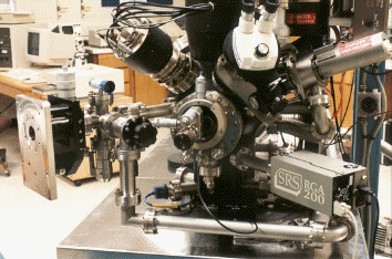
The photograph above shows the high-pressure and temperature cell attached to one of
our UHV multi-technique surface systems, where in-situ alloy wetting under a variety of
conditions can be studied.
use in harsh environment, vehicle, and aircraft applications.
Until recently, there has been widespread, almost exclusive use of tin/lead (Sn/Pb) solder
in the manufacture and assembly of electronic circuit boards. While Sn/Pb solder is
reliable and cost-effective, pending legislation in America, Japan, and Europe to ban or
restrict the use of lead in solder alloys is of vital concern to the electronics industry. Lead
is considered to be a health hazard because of the large history of human lead toxicity
problems and its documented impact on human populations. Given the competitiveness
of the industry and because all equipment and manufacturing requirements have been
based on eutectic Sn/Pb solder, the costs of conversion to a Pb-free solder and its
associated reliability impact are not insignificant.
The goal of our work in this area is to develop a fundamental understanding of alternate
solder alloys that will meet the high volume, high yield, and high reliability assembly
process for automotive electronics. We utilize a broad array of materials, mechanical, and
thermal tests to characterize the solder alloys. A wetting balance allows for measurement
of the adhesive forces during wetting. Video recording and heating capabilities on
SEM/EDX enables in-situ, real-time observation of solder wetting characteristics. A
variable-pressure, bell-jar wetting system allows studies of process gas variations on
solder wetting. A high-pressure, UHV-compatible wetting chamber attached to one of our
surface analysis systems allows us to study the surface physics during solder wetting
and spreading. A torsion oscillating viscosity system enables measurement of solder
viscosity. The oscillating sessile drop method measures solder surface tension.
A unique set of experiments has examined the behavior of the alloys during the wetting
process by dynamic surface chemistry studies of the advancing liquid alloy front. Previous
work using surface techniques such as Auger (AES) and X-ray photoelectron (XPS)
spectroscopies has shown that low-level alloy impurities can segregate to the liquid
surface and cause dramatic changes in wettability. One of our aims is to determine the
critical parameters that affect wetting and provide a comprehensive, atomic-scale picture
of solder wetting phenomena.
The photograph above shows the high-pressure and temperature cell attached to one of
our UHV multi-technique surface systems, where in-situ alloy wetting under a variety of
conditions can be studied.
Wide-Bandgap Electronics
The physical and electronic properties of SiC make it the foremost semiconductor
material for short wavelength optoelectronic, high temperature, radiation resistant, and
high-power/high-frequency electronic devices. Collectively, these properties allow SiC
devices to offer tremendous benefits over other available semiconductor devices in a
large number of industrial and military applications.
We have been engaged in SiC high temperature electronics research for several years.
The focus has been on understanding the behavior of the polar surfaces of SiC as a
function of temperature, metal coverage, and gas reactivity. In addition, we have
elucidated the oxidation mechanisms of SiC faces at the monolayer level, the growth
modes of monolayer coverages of refractory metals on SiC, and the reactive chemistry of
SiC during ohmic and Schottky barrier contact formation.
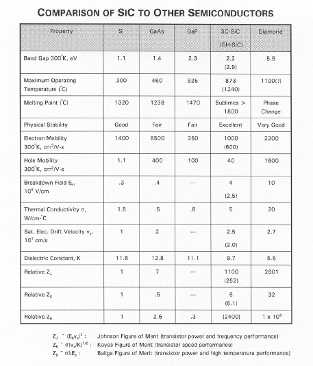
SiC Physical & Electronic Properties
A summary of the most important properties in comparison to Si, GaAs, GaP, and
diamond is shown below:
material for short wavelength optoelectronic, high temperature, radiation resistant, and
high-power/high-frequency electronic devices. Collectively, these properties allow SiC
devices to offer tremendous benefits over other available semiconductor devices in a
large number of industrial and military applications.
We have been engaged in SiC high temperature electronics research for several years.
The focus has been on understanding the behavior of the polar surfaces of SiC as a
function of temperature, metal coverage, and gas reactivity. In addition, we have
elucidated the oxidation mechanisms of SiC faces at the monolayer level, the growth
modes of monolayer coverages of refractory metals on SiC, and the reactive chemistry of
SiC during ohmic and Schottky barrier contact formation.
SiC Physical & Electronic Properties
A summary of the most important properties in comparison to Si, GaAs, GaP, and
diamond is shown below:
Some of our work on SiC surface physics . . .
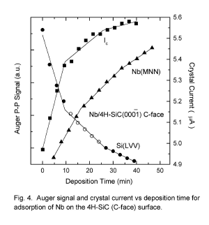
Monolayer Growth Modes of Re and Nb on the Polar Faces of 4H-SiC
K. W. Bryant and M. J. Bozack
Surface Science Laboratory, Department of Physics, Auburn University, Auburn, AL
36849 (USA)
Abstract: Auger electron spectroscopy (AES) and secondary electron emission has been
used to determine how thin monolayer films of Re and Nb grow on the 4H-SiC (C-face)
and 4H-SiC (Si-face) surfaces at room temperature. The secondary electron emission
was monitored by the crystal current (SEECC) method and compared to the change in
Auger electron peak-to-peak intensities for both substrate and adsorbate. On the
4H-SiC (Si-face), both metals first form a single monolayer followed by growth of
simultaneous monolayers (MSM mode). On the 4H-SiC(C-face), both metals grow
layer-by-layer (Frank-van der Merwe, FM mode).
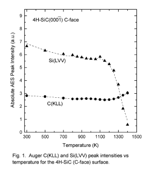
Surface Composition of 4H-SiC as a Function of Temperature
K. W. Bryant and M. J. Bozack
Surface Science Laboratory, Department of Physics, Auburn University, Auburn, AL
36849 (USA)
Abstract: We report surface compositions of the 4H-SiC(C-face) and 4H-SiC (Si-face)
over the temperature range 300 to 1400 K, studied by Auger electron spectroscopy
(AES), energy loss spectroscopy (ELS) and quadrupole mass spectroscopy (QMS).
Below 800 K, no significant changes in surface composition are observed. Between
800 K and 1200 K, silicon preferentially volatilizes, leaving a slightly graphitized
surface. Above 1200 K, preferential volatility of silicon results in a heavily graphitized
surface. The thickness of the graphitized layer is greatest on the 4H-SiC(C-face)
surface (~ 8 Å @ 1400 K). Results are compared with earlier work involving the polar
faces of 6H-SiC.

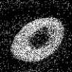
The microstructure of
Sn-3.0Ag-0.5Cu as seen by
scanning electron
microscopy.
Sn-3.0Ag-0.5Cu as seen by
scanning electron
microscopy.

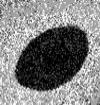
Scanning Auger map for Sn as
Sn-4.0Ag-0.5Cu wets and
spreads over a Pd surface.
Sn-4.0Ag-0.5Cu wets and
spreads over a Pd surface.
Scanning Auger map for Pd as
Sn-4.0Ag-0.5Cu wets and
spreads over a Pd surface.
Sn-4.0Ag-0.5Cu wets and
spreads over a Pd surface.
Scanning Auger map for Ag as
Sn-4.0Ag-0.5Cu wets and
spreads over a Pd surface.
Sn-4.0Ag-0.5Cu wets and
spreads over a Pd surface.